FPCB, PCB Outsourcing
Product Introduction
Application:
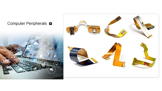
- Computer Peripherals
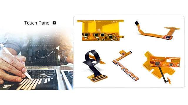
- Touch Pannel
- Automotive Electronics
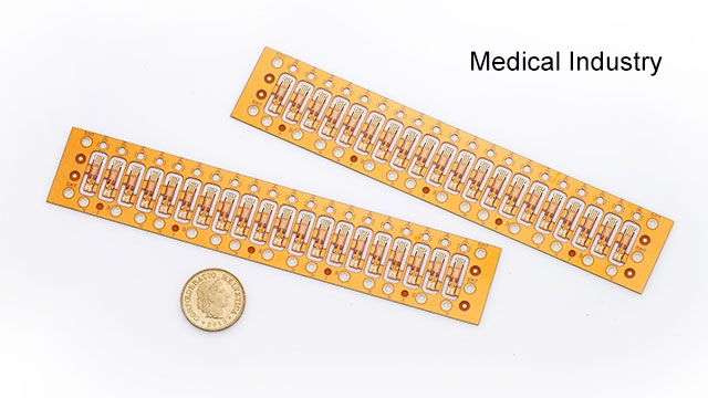
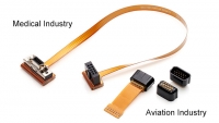
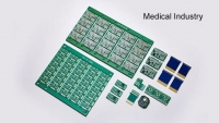
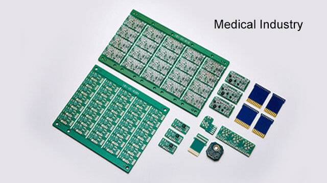
- Medical, Military and Aviation Industry
Manufacturing Capability:
- Multi-layer (up to 36 ) FR4 Rigid PCB with the state of art of techniques. Please refer to the detailed process capabilities as follow charts.
- High Frequency PCBs with low Dk/Df materials of MPI, LCP and BT, and Migration Test.
- Metal-Layer (up to 4) metal based PCBs with aluminum, copper (weight up to 26 oz), Ni-copper, Mn-copper and ion.
- Multi-layer (up to 6) Flex PCB.
- Multi-layer (up to 6 ) rigid flex and flex PCBs.
- “Componentized PCBs including think planar transformer, precious resistor, embedded capacitor and planar inductors.
Flex PCB
| CATEGORY | DESCRIPTION | CAPABILITY |
| Number of Layer | 1 - 6 | 0.1 - 0.4 mm (4-16 mil)+C3:C20 |
| Min. Trace Width/Space | Single Side | 0.030mm (1.2mil)/0.030mm (1.2mil) |
| Double Side/Muti-Sides | 0.035mm (1.4mil)/0.035mm (1.4mil) | |
| Min. Hole Dia | CNC/Laser Drill | 0.1mm (4mil)/0.030 mm (1.2mil) |
| Punch | 0.5mm (20mil) | |
| Surface Treatment | Electro Ni/Au Plating) | Au: 0.025-0.2µm(1-8"µ) Ni: 1.5-20µm (50-500µ") |
| ENEPIG | Au: 0.05-0.15µm(2-6"µ) Pd: 0.05-0.15µm(2-6"µ) Ni: 1.5-20µm (50-500µ") |
|
| ENIG | Au: 0.025-0.1µm(1-4"µ) Ni: 1.5-9µm (50-350µ") |
|
| Dim. Tolerance | Conductor Width | General:±0.02mm, Special:±0.01mm |
| Gold finger Acculate Toleance (Total length ≦ 30 mm) | General:±0.03mm, Special:±0.025mm | |
| Gold finger Acculate Toleance (Total length ﹥30 mm) | General:± Total length*10/10000mm, Special:± Total length*3/10000mm (specified material) |
|
| Min. Pad/Min. Hole Dia. | General: 0.25/0.1 mm (CNC Drill) Special: 0.15/0.03 mm (Laser Drill) |
|
| Outline Dim. | General:±0.1mm, Special:±0.05mm | |
| Gold Finger Shift | General:±0.1mm, Special:±0.07mm | |
| Coverlay Shift | General:±0.2mm, Special:±0.15mm | |
| Hole Dia. | ±0.05mm | |
| Silkscreen printing Shift | General:±0.03mm, Special:±0.25mm | |
| Fold Angle/Stiffener Paste Shift | General:±0.03mm, Special:±0.2mm |
Rigid PCB
| CATEGORY | DESCRIPTION | CAPABILITY | |
| Dimensions | Max. dimensions of product | Testing board:610mmX500mm→Mass:610x500mm | |
| Without Testing board:762mmX620mm→Mass:700x510mm | |||
| PCB Thickness | |||
| Standard thickness | 1.6mm +/- 10% (0.062" +/- 10%) | ||
| Min. thickness | Single/double-side PCB: 0.2mm +/- 0.1mm (0.008" +/- 0.004") | ||
| 4-layer PCB: 0.4mm +/- 0.1mm (0.016" +/- 0.004") | |||
| 6-layer PCB: 0.6mm +/- 0.1mm (0.024" +/- 0.004") | |||
| 8-layer PCB: 0.9mm +/- 0.1mm (0.036" +/- 0.004") | |||
| 10-layer PCB: 1.0mm +/- 0.12mm (0.04" +/- 0.005") | |||
| 12-layer PCB: 1.2mm +/- 0.12mm (0.048" +/- 0.005") | |||
| Max. thickness | 6.0mm +/- 10% | ||
| (0.236" +/- 10% ) | |||
| Warp of PCB | < 7/1000 | ||
| FR-4、High TG FR-4 (170℃/180℃)、ISOLA(FR-408、FR-408HR)、ROGERS、Halogen free、TU(883) | |||
| FR4 thickness (standard) | 1.6mm (0.062") | ||
| Board meaterial | High TG FR4 (170 deg C) (standard) | 1.6mm (0.062") | |
| Metal board | Aluminum substrate, copper substrate | ||
| Max. number of layers | 36 layers | ||
| Cutting | Min. thickness of inner layers | 0.0508mm (0.002") | |
| (excluding copper thickness) | |||
| Minimum size | 0.1mm (0.004") Laser drill, | ||
| 0.15mm(0.006") Mechanical drill→Mass: 0.2mm(0.008") | |||
| Maximum size | 6mm | ||
| Drills | Drill hole deviation | +/- 0.002" (0.050mm) | |
| PTH diameter tolerance | +/- 0.003" (0.075mm) | ||
| Non-PTH diameter tolerance | +/- 0.002" (0.050mm) | ||
| Annual ring isolation | +/- 0.005" (0.127mm) | ||
| Copper plating | Min. hole copper | 0.0008" | |
| Aspect ratio | 1:20 | ||
| Etching | Trace width tolerance | +/- 20% (impedance control +/- 1mil) | |
| Min. trace width/spacing(copper base 1/3oz) | 0.0025"/ 0.0025" (0.064mm)→Mass:0.004"/0.004" | ||
| Min. trace width/spacing(copper base 1/2oz) | 0.005"/ 0.005" (0.13mm) | ||
| Min. trace width/spacing(2oz) | 0.006"/ 0.006" (0.15mm) | ||
| Min. trace width/spacing(3oz) | 0.009"/ 0.090" (0.23mm) | ||
| Min. trace width/spacing(4oz) | 0.013"/ 0.013" (0.33mm) | ||
| MIn. clearance between hole and inner trace | 0.006"(0.15mm) | ||
| Inner layer | Min. inner hole isolatioin ring | 0.006"(0.15mm) | |
| Inter-layer Reqistration | +/- 0.003"(0.08mm) | ||
| Color | Green, Light gree, matt green, white, black, yellow, red, blue, clear | ||
| Solder Mask | Min. space beweent solder mask to make dams | 0.003" | |
| Thickness of solder mask | 0.001" | ||
| Color | White, black, yellow, red, blue, green | ||
| Silkscreen | Min. line width | 0.004" | |
| Min. height/width | 0.024" / 0.032" | ||
| Electro tests | AOI Test | Yes | |
| Flying probe test | Yes | ||
| Impedance control | Tolerance | 5~10% | |
| Impedance tester | POLAR CITS800S4 | ||
| Form and hole expansion | +/- 0.15mm (0.006") | ||
| CNC tolerance | +/- 0.15mm (0.006") | ||
| CNC Routing | V-Cut depth (board th. > =1.0mm ) | +/- 0.1mm (0.004") | |
| V-Cut deviation | +/- 0.1mm (0.004") | ||
| SEMI HOLE | Yes | ||
| Surface treatment | HASL/ Lead-free HASL/ Immersion gold/ Immersion Silver/ Immersion tin/ OSP/ Full (selective)body gold plating/ Gold finger plating/ Carbon ink/ ENEPIG | ||
| Blind buried hole | 3+N+3 | Yes | |
| Via in Pad | Yes | ||


